LIVING LA VIDA LOC(A): A BRIEF INSIGHT INTO THE WORLD OF “LAB ON A CHIP” AND MICROFLUIDICS
Throughout history, humans have always tried to improve the tools they use. Animals were bred to be larger, means of locomotion engineered to become more powerful, etc. Until recently, bigger was thought to be better. However, today it seems the opposite is true: Every day we experience pressure for buying smaller cameras, computers, cell phones, and even cars. It is clear that size reduction is an important facet of our lives.
Obviously, science is inherently involved in this move towards smaller devices. In fact, the word “nano” (a billionth of a standard size) is so hip right now, it seems like any trend-setting scientist should use it with high frequency. And one of the latest developments toward the realm of the small is the so-called “lab on a chip” (LOC) – a device about the size of your palm, able to perform a myriad of tasks associated with a standard laboratory. This idea has been around for a while; and certainly the idea of fitting a lot of equipment on a portable device is convenient, whereby the LOC is envisioned to be a simple tool, that is both easy to operate, and also offers a way to do things where very small amounts of sample are required. As well, such devices are deposable, which make them extremely useful for clinical procedures. For instance, it is possible to conceive of a device that needs only a small sample of bodily fluid to diagnose a patient’s illness. LOC’s are also of great interest to safety and military departments, who would greatly benefit from having portable chemical detection systems.
Although the concept of scaling down a system seems simple, the operation of LOC devices is quite complicated. Different rules apply at small scales: viscous friction (or the resistance to flow) dominates the micro world. The media that a molecule such as a protein moves in, is in effect incredibly dense, because the atomic size of the fluid molecules is comparable in size to the protein itself. Every time a macroscopic object moves, it will displace millions of other molecules in the fluid: but for a microscopic entity dislodging similar sized molecules this movement can be especially challenging. (think of swimming and how you displace the water when you move, and then think of swimming and how you have to displace other swimmers if the pool is very overcrowded). Therefore, gravity and inertial effects no longer matter at this scale. Instead, a molecule has to primarily confront viscous forces and random Brownian motion. For these reasons, the design of a device intended to be very small and yet precise is not easy. From an engineering standpoint, it is essential to keep in mind how differently the system is going to behave compared to the macro scale.
One of the main players in the lab on a chip industry is the microfluidics platform. Micro stands for a unit of measure that is a millionth of the normal scale, i.e. a micrometer is a millionth of a meter. For a sense of scale this is about 100 times smaller than a human hair. The volumes of fluid transported in microfluidic channels can be as little as few nanoliters (a nanoliter corresponds to a billionth of a liter), and sometimes even smaller. In order to handle a large number of samples in small fluid volumes, microfluidic chips contain thousands of channels connected to form a micro fluidic circuit. This setup allows not only the use of tiny reagent volumes but also a high task parallelization since several procedures can processed and physically be fitted on the same chip.
In microfluidic channels the flow of liquid is completely laminar: all of the fluid moves in the same direction and at the same speed. Unlike turbulent flow this allows the transport of molecules in the fluid to be very predictable.
Microfluidic devices are generally made in glass or plastics but several laboratories utilize PDMS, a type of silicone. Some advantages of PDMS are that it is very cheap, optically clear and permeable to several substances, including gases. Since air can quickly diffuse out, the latter aspect is very convenient, making it possible to inject fluid into a channel that has no outlet.
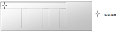
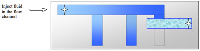
Let’s say we want to make a very simple branched channel, as outlined below.

In this top view, the dark lines represent the flow channels, and let’s define that each channel is to be 100 micrometers wide. First, it should be noted that such features are not very easy to physically carve out in order to make a mold. A machine with high precision on such minute details would be very expensive and would require a lot of time to perform its task. We therefore rely on another method: soft lithography.
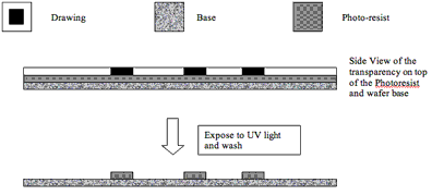
For PDMS devices, soft lithography is based the utilization of substances that become soluble to particular solvents when exposed to UV light. These substances are called photoresists and they appear to be very dense transparent liquids. Upon baking their consistency becomes harder. This technique allows the production of countless features in the same time needed for one (essentially by shining the appropriate pattern of light). Unlike machining the time required does not scale with increased number of elements.
If we were to print the design from the above onto a transparency slide we could use it to make our mold as follows. We can place the slide on top of the baked photoresist (made of the thickness required), and then expose the entire setup to UV light. Under the dark drawing lines the photoresist will not be exposed to the light, while in the exposed areas the photoresist will become vulnerable to the solvent. Upon washing it will dissolve and come off. We will then be left with a cast of the initial design where the dark lines have become solid photoresist 3D lines. You can see that the level of complexity of the chip depends only on the design, and the time required to make the features depends only on the UV scan and the wash step.
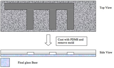
We have now completed the first step towards the fabrication of our chip. If we wanted to add more features to our chip we could do it by following the same procedure as outlined above. We would need to start over with new photoresist. Several layers with different patterns can be made and stacked on top of the previous ones to form a complete microfluidic chip. Layers can be connected vertically by perforating the membrane separating each layer. Of course it is essential to have accurate alignment of each layer. In order to achieve this, alignment marks are made on each one of the layers so that it is possible to position each part correctly.
We are now ready to coat our mold with PDMS – the remaining photoresist lines will become the hollow channels.
The procedure outlined here is a simplification of the protocol used to make microfluidic devices, but it should give you an idea of how the manufacturing works.
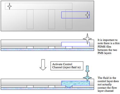
If we wanted to control the fluid through the different channels by forming a valve, we would need to design an additional layer for our chip. For instance, we might want the fluid to go through the third branch only some of the time.
To do this, we can design a control layer and place it in contact with the existing flow layer. If the membrane separating the two layers is thin enough we can easily use the control layer to affect the fluid movement in the flow layer. In fact, if we pressurize a fluid in the control layer the thin PDMS membrane that separates the two layers will deflect and completely block the flow channel.
For the valve to be effective, it is essential that the two layers are separated by a thin membrane: if it was too thick, pressurizing the control channel would not affect the flow layer while if there was no membrane the fluid in the control layer would directly circulate in the flow layer.
The details of fabrication of the control layer are very similar to the ones outlined for the flow layer. When more complicated chips with several layers are made, different types of photoresist are usually employed to vary the thickness or some other property of the layer: the procedure can vary slightly with the different types of materials used.
By combining valves and channels in different configurations, scientists have been able to develop peristaltic pumps, fluid mixers and filters: they have essentially achieved the miniaturization of numerous tools towards the development of the Lab On a Chip. Microfluidic devices are currently employed in a large variety of fields, from medicine to biology and chemistry. Some of the great advantages of these devices lie in operating at such small scales, where experimental sensitivity and precision are much easier to achieve thanks to laminar flow and the well-defined physics of these systems. But even more advantageous is the parallelization that can occur when operating at such small scales. While the amount of reagents needed for the experiments is greatly decreased, the multiplexing of the experiments allows for much higher throughput. These efforts are ultimately resulting in a product that is in very high demand not only in pharmaceutical and biotech research, but also environmental monitoring and security applications.
Hopefully I have convinced you how convenient and widely applicable microfluidic chips are. LOC microfluidic platforms have been used from miniaturized fuel cell to DNA sequencers and it seems like the range of applications is constantly growing. Maybe it won’t be too long until we will all be able to have our own lab on a chip at home: you feel sick one day and maybe you can know what is wrong by simply loading a sample of saliva into a microfluidic device…
BIBLIOGRAPHY AND REFERENCES
1. The S.R. Quake group (assessed November 2006)
2. C L. Hansen et al. 2002. A robust and scalable microfluidic metering method that allows protein
crystal growth by free interface diffusion. PNAS. 26: 16531 – 16536.
3. Stanford Microfluidic Foundry, 2005. “Multilayer Soft Lithography” (Oct 10, 2006)
4. Wikipedia, the free Encyclopedia., 2006. “Lab-on-a-chip” (Oct 2, 2006)
6. Yager Group UW, 2004. “Microfluidic Tutorial – A Highly Biased Primer.” (Sept 30, 2006)